Researchers from Graz University of Technology, Humboldt University in Berlin, M.I.T., Montan University in Leoben and Georgia Institute of Technology report an important advance in the understanding of electrical conduction through single molecules.
Minimum size, maximum efficiency: The use of molecules as elements in electronic circuits shows great potential. One of the central challenges up until now has been that most molecules only start to conduct once a large voltage has been applied. An international research team with participation of the Graz University of Technology has shown that molecules containing an odd number of electrons are much more conductive at low bias voltages. These fundamental findings in the highly dynamic research field of nanotechnology open up a diverse array of possible applications: More efficient microchips and components with considerably increased storage densities are conceivable.
One electron instead of two: Most stable molecules have a closed shell configuration with an even number of electrons. Molecules with an odd number of electrons tend to be harder for chemists to synthesize but they conduct much better at low bias voltages. Although using an odd rather than an even number of electrons may seem simple, it is a fundamental realization in the field of nanotechnology – because as a result of this, metal elements in molecular electronic circuits can now be replaced by single molecules. “This brings us a considerable step closer to the ultimate minitiurization of electronic components”, explains Egbert Zojer from the Institute for Solid State Physics of the Graz University of Technology.
Molecules instead of metal
The motivation for this basic research is the vision of circuits that only consist of a few molecules. “If it is possible to get molecular components to completely assume the functions of a circuit’s various elements, this would open up a wide array of possible applications, the full potential of which will only become apparent over time. In our work we show a path to realizing the highly electrically conductive elements”, Zojer excitedly reports the momentous consequences of the discovery.
Specific new perspectives are opened up in the field of molecular electronics, sensor technology or the development of bio-compatible interfaces between inorganic and organic materials: The latter refers to the contact with biological systems such as human cells, for instance, which can be connected to electronic circuits in a bio-compatible fashion via the conductive molecules.
http://portal.tugraz.at/portal/page/portal/TU_Graz
Single Molecules As Electric Conductors
Clever Acoustics Help Blind People See The World
Video from portable cameras is analysed to calculate the distance of obstacles and predict the movements of people and cars. This information is then transformed and relayed to a blind person as a three-dimensional ‘picture’ of sound.
The concept is apparently simple and two prototypes have been successfully tested. Laser and digital video cameras become the eyes for the blind man and see the objects and activity going on around him.
Researchers from the University of Bristol have developed powerful real-time image processing and some clever algorithms to then identify objects and obstacles, such as trees, street furniture, vehicles and people. The system uses the stereo images to create a “depth map” for calculating distances. The system can also analyse moving objects and predict where they are going.
So much for the image processing, but how do you present this visual information to a blind person? Technology developed at the University of Laguna in Spain makes it possible to transform spatial information into three-dimensional acoustic maps.
A blind person wears headphones and hears how sounds change as they move around. The stereo audio system makes it possible to place sounds so that the brain can interpret them as a point in space. Sounds get louder as you walk towards objects, quieter as you move away. Objects to your right are heard on your right, and if you move your head the sound moves too. And if something is heading right for you, you'll hear it coming, with a tone that tells you to get out of the way.
The full picture
The EU-funded CASBLiP project was conceived to integrate the image processing and acoustic mapping technologies into a single, portable device that could be worn by blind people and help them to navigate outdoors.
The University of Laguna worked to adapt its acoustic mapping system and the University of Bristol refined its image processing algorithms. The device also incorporates a gyroscopic sensor developed by the University of Marche, Italy. This component, called the head-positioning sensor, detects how the wearer moves his head. It feeds back the position of the head and the direction it is facing, so that the relative position of the sounds being played to the wearer also move as expected. For example, if you turn your head towards a sound on the right, the sound must move left towards the centre of the sound picture.
Vision for the future
After three years, the consortium has produced two prototype devices mounted on a helmet. They have been tested successfully in trials by blind people in several real-world environments, including busy streets. Two blind institutions (the German Federation of the Blind and Partially Sighted and the Francesco Cavazza Institute, Italy) were heavily involved in the testing programme.
The first design (M1) uses a laser sensor developed by Siemens and originally intended to detect passengers in cars. It can calculate the distance to objects within 0 to 5m in a 60º field of view. The system is mounted inside glasses and cannot be seen by others because it uses infrared light. The M1 has been extensively tested by blind users who are able to recognise items, such as chairs and trees, from the sound picture they receive.
A second version (M2) adds two digital video cameras to either side of a helmet. It can detect moving objects and predict their path.
The University of Marche has also worked closely with the Cavazza Institute to build a complementary GPS location system. This technology could be used to pinpoint the location of a blind person and integrate the device with additional data sources, such as mapping services. It could provide the wearer with verbal directions to their destination.
“We know that the technology works,” says Guillermo Peris-Fajarnés, who coordinated the project from the Research Group on Graphic Technologies at the Universidad Politecnica de Valencia. “Our tests have been very successful and blind people have been able to navigate comfortably in controlled tests and even along a normal street.”
“There is still a lot of development work to do before this could go on the market, especially to prove that the system is 100% reliable,” Peris-Fajarnés notes. “You can't risk it going wrong while a user is crossing the road.”
He says the consortium has decided to continue work on this aspect beyond the end of the EU funding period.
Nevertheless, Peris-Fajarnés is confident that the device could be commercialised: “We are now looking for manufacturing partners to explore the possibilities for a commercially viable product. There's no other system like this available and it should complement existing aids, such as the white stick. But its commercial success will depend on miniaturising the system and mounting the cameras onto glasses.”
http://cordis.europa.eu./ictresults/
Solar plane to make public debut
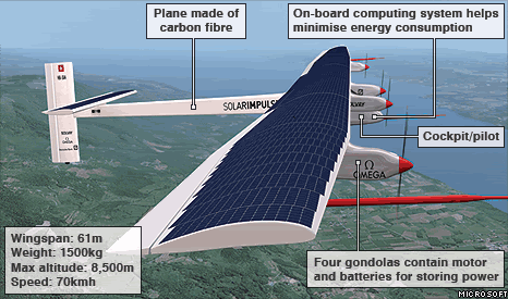
Swiss adventurer Bertrand Picard is set to unveil a prototype of the solar-powered plane he hopes eventually to fly around the world.
The initial version, spanning 61m but weighing just 1,500kg, will undergo trials to prove it can fly at night.
Mr Picard, who made history by circling the globe non-stop in a balloon in 1999, says he wants to demonstrate the potential of renewable energies.
He expects to make a crossing of the Atlantic in 2012.
The flight would be a risky endeavour. Only now is solar and battery technology becoming mature enough to sustain flight through the night - and then only in unmanned planes.
But Picard's Solar Impulse team has invested tremendous energy - and no little money - in trying to find what they believe is a breakthrough design.
"I love this type of vision where you set the goal and then you try to find a way to reach it, because this is challenging," he told BBC News.
Testing programme
The HB-SIA has the look of a glider but is on the scale - in terms of its width - of a modern airliner.
The aeroplane incorporates composite materials to keep it extremely light and uses super-efficient solar cells, batteries, motors and propellers to get it through the dark hours.
Picard will begin testing with short runway flights in which the plane lifts just a few metres into the air.
As confidence in the machine develops, the team will move to a day-night circle. This has never been done before in a piloted solar-powered plane.
HB-SIA should be succeeded by HB-SIB. It is likely to be bigger, and will incorporate a pressurised capsule and better avionics.
It is probable that Picard will follow a route around the world in this aeroplane similar to the path he took in the record-breaking Breitling Orbiter 3 balloon - travelling at a low latitude in the Northern Hemisphere. The flight could go from the United Arab Emirates, to China, to Hawaii, across the southern US, southern Europe, and back to the UAE.
Measuring success
Although the vehicle is expected to be capable of flying non-stop around the globe, Picard will in fact make five long hops, sharing flying duties with project partner Andre Borschberg.
"The aeroplane could do it theoretically non-stop - but not the pilot," said Picard.
"We should fly at roughly 25 knots and that would make it between 20 and 25 days to go around the world, which is too much for a pilot who has to steer the plane.
"In a balloon you can sleep, because it stays in the air even if you sleep. We believe the maximum for one pilot is five days."
The public unveiling on Friday of the HB-SIA is taking place at Dubendorf airfield near Zürich.
"The real success for Solar Impulse would be to have enough millions of people following the project, being enthusiastic about it, and saying 'if they managed to do it around the world with renewable energies and energy savings, then we should be able to do it in our daily life'."
New Technique For Fabricating Nanowire Circuits
Applied scientists at Harvard University in collaboration with researchers from the German universities of Jena, Gottingen, and Bremen, have developed a new technique for fabricating nanowire photonic and electronic integrated circuits that may one day be suitable for high-volume commercial production.
Spearheaded by graduate student Mariano Zimmler and Federico Capasso, Robert L. Wallace Professor of Applied Physics and Vinton Hayes Senior Research Fellow in Electrical Engineering, both of Harvard's School of Engineering and Applied Sciences (SEAS), and Prof. Carsten Ronning of the University of Jena, the findings will be published in Nano Letters. The researchers have filed for U.S. patents covering their invention.
While semiconductor nanowires---rods with an approximate diameter of one-thousandth the width of a human hair---can be easily synthesized in large quantities using inexpensive chemical methods, reliable and controlled strategies for assembling them into functional circuits have posed a major challenge. By incorporating spin-on glass technology, used in silicon integrated circuits manufacturing, and photolithography, transferring a circuit pattern onto a substrate with light, the team demonstrated a reproducible, high-volume, and low-cost fabrication method for integrating nanowire devices directly onto silicon.
"Because our fabrication technique is independent of the geometrical arrangement of the nanowires on the substrate, we envision further combining the process with one of the several methods already developed for the controlled placement and alignment of nanowires over large areas," said Capasso. "We believe the marriage of these processes will soon provide the necessary control to enable integrated nanowire photonic circuits in a standard manufacturing setting."
The structure of the team's nanowire devices is based on a sandwich geometry: a nanowire is placed between the highly conductive substrate, which functions as a common bottom contact, and a top metallic contact, using spin-on glass as a spacer layer to prevent the metal contact from shorting to the substrate. As a result current can be uniformly injected along the length of the nanowires. These devices can then function as light-emitting diodes, with the color of light determined by the type of semiconductor nanowire used.
To demonstrate the potential scalability of their technique, the team fabricated hundreds of nanoscale ultraviolet light-emitting diodes by using zinc oxide nanowires on a silicon wafer. More broadly, because nanowires can be made of materials commonly used in electronics and photonics, they hold great promise for integrating efficient light emitters, from ultraviolet to infrared, with silicon technology. The team plans to further refine their novel method with an aim towards electrically contacting nanowires over entire wafers.
"Such an advance could lead to the development of a completely new class of integrated circuits, such as large arrays of ultra-small nanoscale lasers that could be designed as high-density optical interconnects or be used for on-chip chemical sensing," said Ronning.
The team's co-authors are postdoctoral fellow Wei Yi and Venkatesh Narayanamurti, John A. and Elizabeth S. Armstrong Professor and dean, both of Harvard's School of Engineering and Applied Sciences; graduate student Daniel Stichtenoth, University of Gottingen; and postdoctoral fellow Tobias Voss, University of Bremen.
The research was supported by the National Science Foundation (NSF) and the German Research Foundation. The authors also acknowledge the support of two Harvard-based centers, the National Science Foundation Nanoscale Science and Engineering Center (NSEC) and the Center for Nanoscale Systems (CNS), a member of the National Nanotechnology Infrastructure Network (NNIN).
http://www.fas.harvard.edu/home/
High-speed Integrated Nanowire Circuits
Chemists and engineers at Harvard University have made robust circuits from minuscule nanowires that align themselves on a chip of glass during low-temperature fabrication, creating rudimentary electronic devices that offer solid performance without high-temperature production or high-priced silicon.
The researchers, led by chemist Charles M. Lieber and engineer Donhee Ham, produced circuits at low temperature by running a nanowire-laced solution over a glass substrate, followed by regular photolithography to etch the pattern of a circuit. Their merging of low-temperature fabrication and nanowires in a high-performance electronic device is described this week in the journal Nature.
"By using common, lightweight and low-cost materials such as glass or even plastic as substrates, these nanowire circuits could make computing devices ubiquitous, allowing powerful electronics to permeate all aspects of living," says Lieber, the Mark Hyman Jr. Professor of Chemistry in Harvard's Faculty of Arts and Sciences. "Because this technique can create a high-quality circuit at low temperatures, it could be a technology that finally decouples quality electronics from single crystal silicon wafers, which are resilient during high-temperature fabrication but also very expensive."
Lieber, Ham and colleagues used their technique to produce nanowire-based logical inverters and ring oscillators, which are inverters in series. The ring oscillator devices, which are critical for virtually all digital electronics, performed considerably better than comparable ring oscillators produced at low temperatures using organic semiconductors, achieving a speed roughly 20 times faster. The nanowire-derived ring oscillators reached a speed of 11.7 megahertz, outpacing by a factor of roughly 10,000 the excruciatingly slow performance attained by other nanomaterial circuits.
"These nanowire circuits' performance was impressive," says Ham, assistant professor of electrical engineering in Harvard's Division of Engineering and Applied Sciences. "This finding gives us confidence that we can ramp up these elementary circuits to build more complex devices, which is something we now plan to do."
Lieber and Ham say these functional nanowire circuits demonstrate nanomaterials' potential in electronics applications. The circuits could be used in devices such as low-cost radio-frequency tags and fully integrated high-refresh-rate displays, the scientists write in Nature; on a larger scale, such circuits could provide a foundation for more complex nanoelectronics. The technique Lieber and Ham used to produce a nanowire-based circuit on a glass substrate is also compatible with other commonplace materials such as plastics, broadening its potential applicability.
http://www.harvard.edu/
Scientists Engineer Cellular Circuits That Count Events
MIT and Boston University engineers have designed cells that can count and "remember" cellular events, using simple circuits in which a series of genes are activated in a specific order.
Such circuits, which mimic those found on computer chips, could be used to count the number of times a cell divides, or to study a sequence of developmental stages. They could also serve as biosensors that count exposures to different toxins.
The team developed two types of cellular counters, both described in the May 29 issue of Science. Though the cellular circuits resemble computer circuits, the researchers are not trying to create tiny living computers.
"I don't think computational circuits in biology will ever match what we can do with a computer," said Timothy Lu, a graduate student in the Harvard-MIT Division of Health Sciences and Technology (HST) and one of two lead authors of the paper.
Performing very elaborate computing inside cells would be extremely difficult because living cells are much harder to control than silicon chips. Instead, the researchers are focusing on designing small circuit components to accomplish specific tasks.
"Our goal is to build simple design tools that perform some aspect of cellular function," said Lu.
Ari Friedland, a graduate student at Boston University, is also a lead author of the Science paper. Other authors are Xiao Wang, postdoctoral associate at BU; David Shi, BU undergraduate; George Church, faculty member at Harvard Medical School and HST; and James Collins, professor of biomedical engineering at BU.
Learning to count
To demonstrate their concept, the team built circuits that count up to three cellular events, but in theory, the counters could go much higher.
The first counter, dubbed the RTC (Riboregulated Transcriptional Cascade) Counter, consists of a series of genes, each of which produces a protein that activates the next gene in the sequence.
With the first stimulus — for example, an influx of sugar into the cell — the cell produces the first protein in the sequence, an RNA polymerase (an enzyme that controls transcription of another gene). During the second influx, the first RNA polymerase initiates production of the second protein, a different RNA polymerase.
The number of steps in the sequence is, in theory, limited only by the number of distinct bacterial RNA polymerases. "Our goal is to use a library of these genes to create larger and larger cascades," said Lu.
The counter's timescale is minutes or hours, making it suitable for keeping track of cell divisions. Such a counter would be potentially useful in studies of aging.
The RTC Counter can be "reset" to start counting the same series over again, but it has no way to "remember" what it has counted. The team's second counter, called the DIC (DNA Invertase Cascade) Counter, can encode digital memory, storing a series of "bits" of information.
The process relies on an enzyme known as invertase, which chops out a specific section of double-stranded DNA, flips it over and re-inserts it, altering the sequence in a predictable way.
The DIC Counter consists of a series of DNA sequences. Each sequence includes a gene for a different invertase enzyme. When the first activation occurs, the first invertase gene is transcribed and assembled. It then binds the DNA and flips it over, ending its own transcription and setting up the gene for the second invertase to be transcribed next.
When the second stimulus is received, the cycle repeats: The second invertase is produced, then flips the DNA, setting up the third invertase gene for transcription. The output of the system can be determined when an output gene, such as the gene for green fluorescent protein, is inserted into the cascade and is produced after a certain number of inputs or by sequencing the cell's DNA.
This circuit could in theory go up to 100 steps (the number of different invertases that have been identified). Because it tracks a specific sequence of stimuli, such a counter could be useful for studying the unfolding of events that occur during embryonic development, said Lu.
Other potential applications include programming cells to act as environmental sensors for pollutants such as arsenic. Engineers would also be able to specify the length of time an input needs to be present to be counted, and the length of time that can fall between two inputs so they are counted as two events instead of one.
They could also design the cells to die after a certain number of cell divisions or night-day cycles.
"There's a lot of concern about engineered organisms — if you put them in the environment, what will happen?" said Collins, who is also a Howard Hughes Medical Institute investigator. These counters "could serve as a programmed expiration date for engineered organisms."
The research was funded by the National Institute of Health Director's Pioneer Award Program, the National Science Foundation FIBR program, and the Howard Hughes Medical Institute.
http://web.mit.edu/
Superconducting Chips To Become Reality
Most chemical elements become superconducting at low temperatures or high pressures, but until now, copper, silver, gold, and the semiconductor germanium, for example, have all refused superconductivity. Scientists at the Forschungszentrum Dresden-Rossendorf (FZD) research center were now able to produce superconducting germanium for the first time. Furthermore, they could unravel a few of the mysteries which come along with superconducting semiconductors.
Superconductors are substances that conduct electricity without losses when cooled down to very low temperatures. Pure semiconductors, like silicon or germanium, are almost non-conducting at low temperatures, but transform into conducting materials after doping with foreign atoms. An established method of doping is ion implantation (ions = charged atoms) by which foreign ions are embedded into the crystal lattice of a semiconductor. To produce a superconducting semiconductor, an extreme amount of foreign atoms are necessary, even more than the substance would usually be able to absorb. At the FZD, germanium samples were doped with about six gallium atoms per 100 germanium atoms. With these experiments, the scientists could prove indeed that the doped germanium layer of only sixty nanometers thickness became superconducting, and not just the clusters of foreign atoms which could easily form during extreme doping .
As the germanium lattice is heavily damaged by ion implantation, it has to be repaired afterwards. For such purposes, a flash-lamp annealing facility has been developed at the FZD. Its application allows for a repair of the destroyed crystal lattice by rapidly heating the sample surface (within few milliseconds) while the distribution of the dopant atoms is kept almost the same.
From a scientific point of view, the new material is very promising. It exhibits a surprisingly high critical magnetic field with respect to the temperature where the substance becomes superconducting. For many materials, superconductivity occurs only at very low temperatures, slightly above the absolute zero point of -273 degrees Celsius or 0 Kelvin. The gallium doped germanium samples become superconducting at about 0.5 Kelvin; however, the FZD researchers expect the temperature to increase further by changing various parameters during ion implantation or annealing.
Physicists have been dreaming about superconducting semiconductors for a long time, but saw only few chances for the semiconductor germanium to become superconducting at all. Germanium used to be the material for the first generation of transistors; however, it was soon replaced by silicon, the current material for microelectronics. Recently, the “old” semiconductor material germanium has aroused more and more interest, as it allows, compared to silicon, for more rapid circuits.
Experts even believe germanium to be rediscovered for micro- and nanoelectronics. The reason for such a renaissance lies in the fact that miniaturization in microelectronics industry using silicon is coming to an end. Today, extremely thin oxide layers are needed for transistors, down to a level where silicon oxide does not work well any more. Germanium as a new material for chips would come along with two big advantages: it would enable both faster processes and further miniaturization in micro- and nanoelectronics. Superconducting germanium could thus help to realize circuits for novel computers.
The scientists at the Forschungszentrum Dresden-Rossendorf followed a targeted approach when searching for a new superconducting semiconductor. Instead of doping with boron, which had resulted in superconducting silicon two years ago in France, the scientists choose gallium because of its higher solubility in germanium. In many systematic experiments they proved that the superconductivity of germanium can be reproduced. Furthermore, they were able to show that the transition temperature marking the start of superconductivity can be raised within certain limits.
In the future, the scientists at the two FZD institutes “Ion Beam Physics and Materials Research” and “Dresden High Magnetic Field Laboratory” will combine their know-how in order to fine-tune different rather complex parameters for further experiments, thus hopefully discovering further mysteries of superconducting semiconductors.